1682 Logic level fiber optic serial interface

- SKU:
- 1682

Description
The 1682 fiber optic to logic level RS232 serial interface uses Broadcom transmitters and receivers to provide a high speed full duplex communication channel with the ultimate in galvanic isolation. This interface is perfect for remote control for high voltage systems or control of ground-isolated RF systems. A complete computer controlled data link can be implemented when this module is paired with the 1505 USB to fiber module which enumerates as a virtual com port.
Accessories:
- 1505 USB to serial fiber optic interface
- Friction latched duplex fiber optic cable
- Latching duplex fiber optic cable
Serial specifications:
- Full duplex operation using duplex fiber.
- Protocol agnostic, i.e. start, data parity and stop bits are not controlled by this interface.
- Interface optimized for 115.2kbps with a 100M cable run with properly terminated optical cable/connectors.
- Longer runs at lower baud rates or shorter runs with higher baud rates possible.
- The module consumes 20mA max during idle, the transmit LED is off during data idle (High logic level).
Transmit power:
- The transmitter LED current is set to the maximum current of 30mA using a 100 ohm 2010 (1/2W) resistor at R1.
- The current can be set to lower values to support shorter cable runs or lower baud rates by changing the value of R1.
- R1 = (5V-1.5V)/IF: For 15mA R1 would be 230 ohms.
- Maximum data rate in all cases is limited to 10Mbps although the practical limit for asynchronous RS232 is 460.8kbps to maintain the specification's sample point requirements.
Input power:
- The logic interface that powers the RXD and TXD buffers operates independently of VCC and VIN and has an input range of 1.65 to 5.50V.
- VCC may be used to power the optical interface (VIN open) with a range of 4.50 to 5.50V.
- VIN may be used to power the optical interface (VCC open or loaded) with a range of 5.40 to 26.0V.
- When powered from VIN, VCC is a regulated 5.0V that may be loaded up to 300mA.
- VIN is tolerant of inputs down to -20V and transients up to +60V. Positive transients must be limited to <100mS and <1% duty cycle typical of an automotive load dump situation.
- Input current 20mA (Idle) and 50mA (Transmitting) with the standard 100 ohm R1.
VIN considerations:
- The on board regulator from VIN to VCC has a thermal resistance θjc of 15°C/W with a maximum junction temperature of 125°C.
- Input voltage and load current at VCC must be limited to ensure the junction temperature does not exceed the limit during the worst case transmit duty cycle.
- The regulator is thermally protected and will shut down if its junction temperature is exceeded.
- The regulator is load protected and will fold back its voltage if its current limit is exceeded.
Interface connector: JST PHR-6
- Provided with a 12 inch ribbon cable terminated with the required PHR-6 connector
- 1 Ground
- 2 RXD (Received bits out of module into processor RXD)
- 3 TXD (Transmitted bits into module out of processor TXD)
- 4 VIO (1.65 to 5.50V for RXD and TXD interface)
- 5 VCC (4.50 to 5.50V for optical interface. May be loaded to 300mA when VIN supplied)
- 6 VIN (5.40 to 26V alternative input to supply VCC with 5.00V)
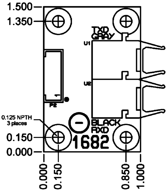
Mechanical outline:
Related Products
Related Products


1505C3 - Optical cable assembly with latching connectors
$4.00
Duplex optical fiber terminated on one end with a friction lock connector and on the other end with a latching connector.
Features:

1505C2 - Optical cable assembly with latching connectors
$4.00
Duplex optical fiber terminated on both ends with latching connectors.
Features:
Latching connectors are compatible with the 1